The VLSI Design Flowchart: A Complete Information
Associated Articles: The VLSI Design Flowchart: A Complete Information
Introduction
With nice pleasure, we are going to discover the intriguing subject associated to The VLSI Design Flowchart: A Complete Information. Let’s weave attention-grabbing data and provide contemporary views to the readers.
Desk of Content material
The VLSI Design Flowchart: A Complete Information
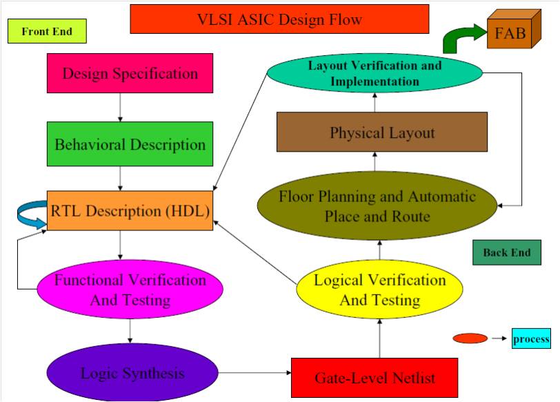
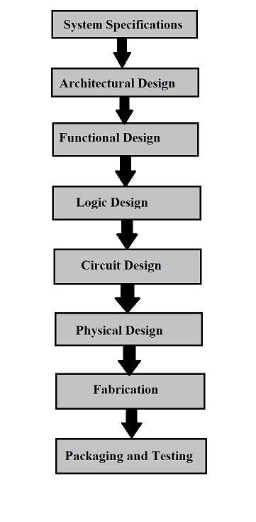
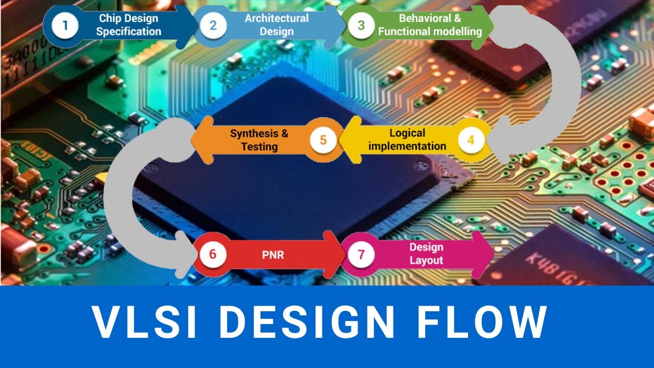
Very-Giant-Scale Integration (VLSI) design is a fancy course of involving the creation of built-in circuits (ICs) with thousands and thousands and even billions of transistors. The design move, from preliminary idea to closing manufactured chip, is intricate and requires a scientific method. This text particulars a complete VLSI design flowchart, explaining every stage and its significance.
I. System-Degree Design:
This preliminary part focuses on defining the general performance and specs of the chip. It is essential to ascertain clear targets earlier than delving into the lower-level design particulars.
-
1.1 System Specification: This includes defining the system’s meant performance, efficiency necessities (pace, energy consumption, space), enter/output interfaces, and different constraints. This stage typically includes making a high-level block diagram illustrating the main elements and their interactions. Detailed specs are essential to information subsequent design decisions.
-
1.2 Algorithm Design & Verification: As soon as the system’s performance is specified, algorithms to implement the specified capabilities are designed. This includes deciding on acceptable algorithms and knowledge constructions, contemplating components like computational complexity and useful resource utilization. Simulation and verification at this stage are important to make sure the algorithm’s correctness and feasibility. MATLAB or comparable instruments are continuously used for algorithm prototyping and verification.
-
1.3 System Structure Design: This part interprets the high-level system specification right into a extra concrete structure. It includes partitioning the system into smaller, manageable modules, defining their interfaces, and deciding on acceptable architectures for every module (e.g., pipelined, parallel). This stage typically includes exploring totally different architectural choices and evaluating their trade-offs when it comes to efficiency, energy, and space. {Hardware} Description Languages (HDLs) like SystemVerilog or VHDL is perhaps launched at this stage for high-level modeling.
II. RTL Design & Verification:
This part includes translating the system structure into Register-Switch Degree (RTL) descriptions utilizing HDLs. RTL describes the info move and management move inside the system at a better stage of abstraction than the gate stage.
-
2.1 RTL Coding: Utilizing HDLs (VHDL or Verilog), designers describe the performance of every module when it comes to registers, combinational logic, and their interconnections. This stage requires a deep understanding of HDL syntax and greatest practices. Effectively-structured, modular code is essential for maintainability and verification.
-
2.2 RTL Simulation & Verification: As soon as the RTL code is written, it is rigorously simulated to confirm its performance towards the system specs. This includes creating testbenches that apply numerous enter stimuli and verify the outputs towards anticipated outcomes. Superior verification strategies like constrained random verification and formal verification are employed to make sure complete protection. Simulation instruments like ModelSim or VCS are generally used.
-
2.3 Synthesis: Synthesis is the method of translating the RTL code right into a gate-level netlist. This includes mapping the RTL constructs onto a goal know-how library, optimizing the design for space, energy, and efficiency. Synthesis instruments like Synopsys Design Compiler are used to automate this course of. Constraints are specified to information the synthesis course of, guaranteeing the design meets the desired necessities.
III. Logic Synthesis & Optimization:
This part focuses on optimizing the gate-level netlist generated from RTL synthesis.
-
3.1 Logic Optimization: The synthesized netlist is optimized to scale back space, energy consumption, and demanding path delay. This includes strategies like gate sizing, buffer insertion, and logic restructuring. Optimization instruments inside the synthesis software or devoted logic optimization instruments are employed.
-
3.2 Static Timing Evaluation (STA): STA verifies that the timing constraints are met within the optimized netlist. It analyzes the propagation delays via the gates and interconnects to determine any timing violations. STA instruments assist determine crucial paths and information additional optimization efforts.
IV. Bodily Design:
This part interprets the optimized netlist right into a bodily structure on the silicon die.
-
4.1 Floorplanning: This includes arranging the main blocks of the design on the chip, contemplating components like space, energy distribution, and sign routing. Floorplanning instruments assist automate this course of.
-
4.2 Placement: This stage includes assigning particular places on the chip to every gate and interconnect. Placement instruments intention to reduce wire size and optimize sign routing.
-
4.3 Routing: This includes creating the bodily interconnections between the gates and blocks. Routing instruments be certain that all alerts are linked accurately and that the routing does not violate design guidelines.
-
4.4 Bodily Verification: After routing, bodily verification ensures the structure meets all design guidelines and specs. This includes checks for design rule violations (DRC), quick circuits, and open circuits. Format versus schematic (LVS) checks confirm that the bodily structure precisely displays {the electrical} schematic.
V. Fabrication & Testing:
-
5.1 Fabrication: The finalized structure is distributed to a fabrication facility (fab) the place the chip is manufactured. This includes a number of steps together with photolithography, etching, ion implantation, and metallization.
-
5.2 Testing: After fabrication, the chips are examined to confirm their performance and determine any defects. This includes making use of numerous take a look at patterns and checking the outputs. This stage consists of each practical testing and parametric testing.
VI. Submit-Silicon Validation:
- 6.1 Submit-Silicon Validation: Even after rigorous testing, there is perhaps discrepancies between the simulated habits and the precise chip habits. Submit-silicon validation includes evaluating the chip’s efficiency with the specs and figuring out any discrepancies. This may contain debugging, additional optimization, and even design revisions.
Flowchart Illustration:
A simplified flowchart illustration would appear to be this:
[System-Level Design] --> [RTL Design & Verification] --> [Logic Synthesis & Optimization] -->
[Physical Design] --> [Fabrication & Testing] --> [Post-Silicon Validation]
Every of those main levels could be additional damaged down into smaller sub-stages, as detailed above. The complexity of the flowchart and the instruments used will fluctuate relying on the scale and complexity of the VLSI design. Trendy VLSI design depends closely on Digital Design Automation (EDA) instruments to automate many of those steps. Nevertheless, human experience stays essential all through the whole course of, significantly in decision-making, problem-solving, and verification. A powerful understanding of the VLSI design move is crucial for anybody concerned on this difficult and rewarding discipline. The iterative nature of the design course of also needs to be famous; suggestions loops exist between levels, permitting for design refinements primarily based on simulation outcomes and verification checks. This ensures that the ultimate product meets the desired necessities and performs optimally.


Closure
Thus, we hope this text has supplied beneficial insights into The VLSI Design Flowchart: A Complete Information. We hope you discover this text informative and helpful. See you in our subsequent article!